Antminer S19j pro aluminum board repair guide
-
Ⅰ. Repair platform / Tools / Equipment Preparation
1. Platform requirements
A grounded anti-static maintenance workbench is required, and maintenance personnel must wear anti-static wrist straps.
2. Equipment requirements
(1) Constant temperature soldering iron (350°C-380°C / 662°F-716°F) and pointed soldering iron for soldering SMD resistors, capacitors and other small patches.
(2) Heat guns, heating (350°C-400°C) and BGA rework stations for chip and BGA desoldering and welding.
(3) A multimeter (Fluke is recommended) with welded steel needle and heat-shrinkable sleeve for easy measurement.
(4) Oscilloscope.
(5) Network cable (requirement: stabilizing Internet network).
3. Test Tool Requirements
Use APW12 power supply to build a test platform (Recommended to use APW12 12V-15V V1.2 and power adapter cable):
(1) Use thick copper wires to connect the positive and negative poles of the PSU and the hash board. It is recommended to use 4AWG copper wires with a length less than 60cm (only for PT1 and maintenance tests), which can be used to power the hashboard.
(2) Use the V2.2010 control board test fixture (model ZJ0001000001), and the positive and negative poles of the power supply need to be equipped with discharge resistors. It is recommended to use 20 ohm cement resistors above 100W; or you can also use the PicoBT multi-function test jig.
4. Repair auxiliary materials and tools requirment
(1) SENJU solder paste M705, flux, hash board cleaner, anhydrous alcohol, thermal conductivity gel, implant ball stencil (66 chip size), suction solder wire, tin ball (recommended diameter 0.4mm).
(2) Circuit board cleaners for cleaning flux residues after repairs;
(3) After maintenance, apply FujipolySPG-30B thermal grease on the surface of the chip;
When replacing a new chip, it is necessary to tin-plant the pins of the chip first, then solder it to the hash board, and evenly apply thermal conductive silicone grease on the surface of the chip, and finally install the large heat sink.
(4) ZD2200 Wired Scanner
(5) TTL to RS232 serial port module
(6) Self-made short-circuit probe (large-headed needle wiring is used for soldering, and it is required to heat shrink sleeve to prevent the probe and small heat sink short circuit.)
5. Common maintenance spare materials:
0402 resistors: 0R, 33R, 51R, 10K, 4.7K
0402 capacitance: 0.luF, luF
Ⅱ. Operation Requirements
1. Maintenance personnel must have certain electronic knowledge, more than one year of maintenance experience, and be proficient in BGA/OFN/LGA packaging welding technology.
2. The repaired hash board must pass two or more tests before it can be qualified.
3. When replacing the chip, pay attention to the operating specifications, ensure that the PCB board is not deformed after replacing the parts, and check whether there are missing parts, open circuit and short circuit around the replaced parts.
4. To test the replaced chip, test the chip first, and then perform the functional test (PT2). Ensure that the small heatsink soldering is OK and large thermal instalation in place (each thermal adhesive must be applied evenly after the installation of a large heatsink). and the cooling fan is at full speed. To use chassis for cooling, it is required to put 2 pieces of hashboard at the same time to form a duct, which is also required (and important) for the single-sided test of production.
5. To power on hash board, put the negative and positive copper wire in place in sequence, and finally the signal cable. Removal must be performed in the reverse order, ie. removing the signal cable, followed by the positive and negative copper wire of power supply Failure to follow this order may cause U1 and U2 damage (failure to find the chip in complete). Before pattern test, the repaired hash board must be cooled down before testing, otherwise it will lead to test PNG.
6. Confirm the miner needs to be repaired, the corresponding test software parameters and test fixture.
7. Check the tools and fixture whether they can work properly.
8. Fans are used for cooling purpose when measuring signals, so it is required to keep 4 fans running at full speed.
9. Replace the new chip to clean the pins and apply solder paste to ensure that the chip is coated with tin before soldering.
Ⅲ. Fixture Setup and Precautions
1. Fixture model: ZJ0001000001
2. For the first time to use S19j pro series, complete FPGA for the fixture control board with test fixture SD card swiping program, unzip and copy to SD card, the memory card fixture card slot. Power on for about 1 minute and wait for the control board indicator to double flash 3 times after the is completed (failure to may cause the reporting of a bad chip during test).
3. Setup of SD card without heat sink: repair using REPALR's program, the following screenshot ilustrates that this program does not need to scan the code. During measurements, heat dissipation is required for PCBA, in order to prevent the test, measurement process board overheating.
4. Setup of SD card without heatsink: The double-sided heatsink 8 x Pattern test requires the setup of SD cards, as indicated below. Change the file name "congfig ini-BHB42631-PT2" to "config ini". PT2 test can be conducted without ing the code scanner, only ing the network cables. For heat dissipation, please refer to the setup of heat dissipation tool (Essentials: the board is ed the chassis, lock screw for power supply, fans need to be at full speed with ambient temperature less than 30 °C).
IV. Principle and Structure of Hash board
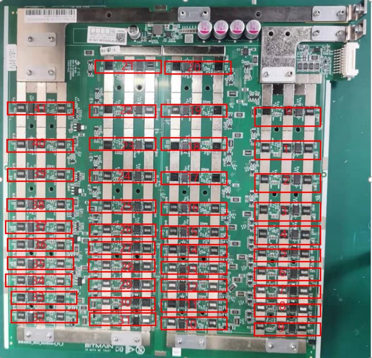
1.Working structure of S19j pro hash board
The hash board consists of 126 BM1362 chips, divided 42 domains, each comprising 3 ASIC chips. The BM1362 chips used in the S19J Pro hash board operate at 0.32V.
The 42nd, 40th, 38th and 36th groups (4 groups in total) are powered by the 20V output from the boost circuit U238 to the LD0 (U308, U305, U306 and U307), so that the LDO of these 4 domains outputs 1.2V and 0.8V. The remaining domain LDO's are powered by VDD15V input, making them output 1.2V and 0.8V.
Attention: PT2 test, we can view on the back-end log page and start counting from asic0, as shown below:
The voltage domain in the test log is counted from 0, i.e. domain0, as shown below:
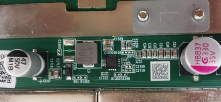
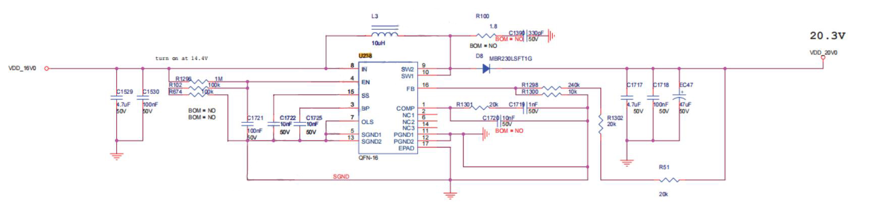
2. S19j pro hash board boost circuit, which will boost the power from 15V to 20V. As showing:
3. Signal direction of S19J PRO chip.
(1) CLK (XIN) signal flow: generated by the Y125M crystal, transmitted from chip 01 to 126; voltage is about 0.5V-0.6V.
.
.
.
Download, you can view all S19xp hash board repair guides.
As a student of ZMRC crypto miner repair academy, you can download this Bitmain S19xp maintenance tutorial for free.
Click To Obtain